
Max Simmonds
M.Eng (Hons) First Class
Software engineer at Starship Technologies and co-founder of Purple Parrot. Previously at CERN and ESA. MEng (Hons, 1st) from the University of Plymouth. Based in Tallinn, Estonia.
Project Status
LED Streaming Display - Rocket Countdown
02/02/26
Requirements
Okay, so, as I said. I want to have a scrolling LED, wall mounted display that can show:
- Temperature
- Time
- Date
- Latest Rocket Launch
- Other stuff
Basically, anything that I want to put on it. It’ll be Wi-Fi enabled (either by ESP32, or RPI or something, not yet decided. If I can get away with the low pin count of the ESP, then that makes the most sense).
In terms of loose requirements, in no particular order:
- Should be made as cheaply as possible. That means using whatever I have to hand, and buying very little extra
- I want quite a few modules. About 10-15. So buying the standard 8x8 modules, and the MAX7219 (almost 20€ or so each!)
- 1xn is required. 2xn might be possible, but maybe left for the future.
- Single colour LEDs, (RED). Future project could utilise RGB, and/or single wire protocol, addressable.
- USB powered
- Easily readable from a few meters. That means large modules, and enough of them to make readability better.
- Be able to make some noise. I think a simple buzzer would suffice initially, maybe there’s scope for a speaker, but to have an alarm or stopwatch, I want it to make some noise.r a speaker, but to have an alarm or stop watch function then I want it to make some noise.
- Easily be able to update the display, so needs some sort of UI. I want to be able to do this from my phone and or laptop.
The main parts of the design will be:
- Plastic enclosure module 1.1 Will be 3D printed. Designed in either Onshape or Freecad (preferably the former if my free period is still available)
- Electronics 2.1 Some type of power supply - could be directly from USB, I don’t anticipate the current to be too high, I’ll be driving one column at a time (will need to check if I can keep the refresh rate >50Hz with a 15 module long display while keeping the brightness reasonable). 2.2 Controller - so this will be something like ESP32, or RPI (something with Wi-Fi) 2.3 Driver - now this is were the project gets interesting. A simple solution is to buy 15 MAX7219’s, that’s like \(15 x 20 = £300\) !!! And that’s before we add the rest of the stuff in. Likely I will be charliplexing this, rather than simple x/y multiplexing. That’ll save me some pins, at the expense of software complexity (but hey, bits are free!). I’m thinking of something like shift registers, maybe some IO expanders, I’m not sure yet. But this will be the problem we need to solve first, and it’ll drive the constraints.
- UI - this will be pretty simple, so doesn’t warrant much here.
That’s all for now, tomorrow we’ll tackle the multipl>exing issue!
07/02/26
Okay, so it’s been a little longer than “the next day”. I should have known. I’ve been busy on a few projects in parallel (I have a startup utilising edge AI, an enclosure for my 3D printer, and a few others in the works).
Anyway, I’ve been googling and thinking about multiplexing vs charlieplexing. I read some interesting pros and cons. Originally, I wanted to go with the former, as I was thinking __“damn if I want 15 or so modules, with 64 LEDS each, that’s almost 1000 LEDs. Each requiring a driving pin. No microcontroller has that many pins.
I was thinking of solutions with charlieplexing, shift registers, I2C IO expanders, and then I realised, there’s no point charlieplexing (which has downsides in refresh rates and brightness, plus ‘ghosting’ issues between switching), I was going to have to use shift registers in any case, so IO expanders were not really needed (can daisy chain the shift registers). The added complexity of charliplexing (which needs tristate shift registers) was just not needed.
With 3 pins:
- Data
- Strobe
- Clock
I can drive any number of LEDs with just these three DIO pins - I can add more whenever I want (just software update) and I can still scroll either vertically or horizontally. So this really seems like the best of all worlds.
Each shift register output needs to be able to drive the LED and sink current from it. Typically, this is about 25mA for full brightness. We can PWM LEDs on a “per module” basis using the output enable (OE) pin on the shift register (obviously, we’ll need to choose one that has this feature, I have 3 in mind, which I’ll show a pro/con for each, but likely we will settle for the simple 74HC595).
This means we can easily use the ESP32, and run as many 8x8 modules that we need.
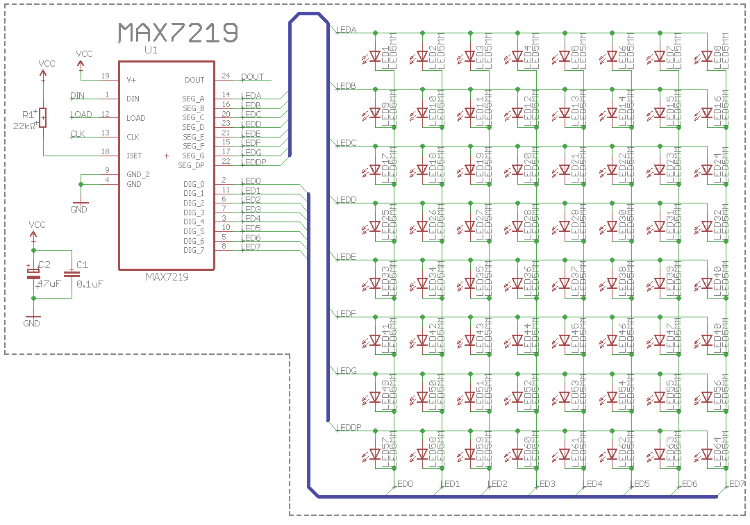
The Shift Register
A lot of this project is defined by the shift register choice. I’ve been looking around, asking Gemini, etc., and I think I’ve come to a decision. The 4 I thought about were:
- CD4014
- 74HC595
- TPIC6B595
- MAX7219
The winner, based on price and a few other things, was the 74HC959. Let’s summarise them below:
| IC | Pros | Cons | Price |
|---|---|---|---|
| CD4014 | • Cost is essentially €0 (I have 4) • Good for learning |
• PISO (Parallel-In, Serial-Out) is the opposite of what we want • No output latch (flicker) |
~€1-2 |
| 74HC595 | • OE pin allows for PWM • Extremely cheap |
• 6mA limit! Needs a Darlington array (ULN2803) or external transistors to handle the current | ~€0.20 |
| TPIC6B595 | • 150mA per output (massive) • Power shift register |
• More expensive • Harder to source on LCSC |
~€1.00 |
| MAX7219 | • Purpose-built display driver • Built-in multiplexing • LCSC Chinese clones make it affordable |
• Genuine Maxim versions are crazy expensive (€15+) • Requires 10µF/0.1µF caps to stay stable |
~€1.00 |
So, let’s think, maybe we should go with the MAX7219? Let’s think more about this tomorrow.
10/02/26
Okay, a few days late but hey, we’re back. Let’s pick up where we last were, I think the MAX7219 is the choice. Specifically, the MAX7219M/TR. For each module (64 LEDs), I would need only 1 for each 8x8 module. That’s pretty good. Also, it’s possible to control the brightness digitally too. Finally, they can be cascaded - so that works well for this scrolling text.
The LEDs
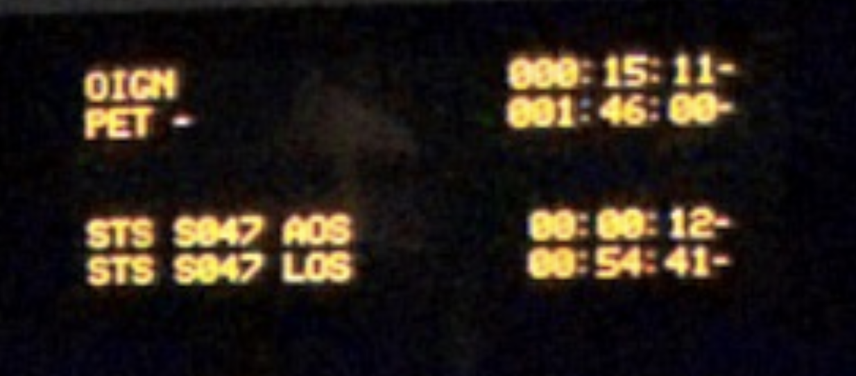
So, next step is to take a look at some LEDs. We’re going to need a lot, so I want some cheap ones. I’m not too sure on size yet, either. I’m not sure if I need SMD or THT - I’m inclinded to thing that THT would be more the look I’m going for. From NASAs mission control center:
Looking on LCSC this LED looks to be a good fit. In 1000 quantities, it’s about $27.7. That’s not too bad, so probably will get these. They’re clear (which probably looks better when LEDs are off) and then it’s green when it’s on.
21/02/26
Well it’s been a little while, but I have been working (I promise). I’ve been getting the base schematic done, I won’t share it just yet, I’ll wait till it’s done. But here’s a few insights I’ve gotten so far:
-
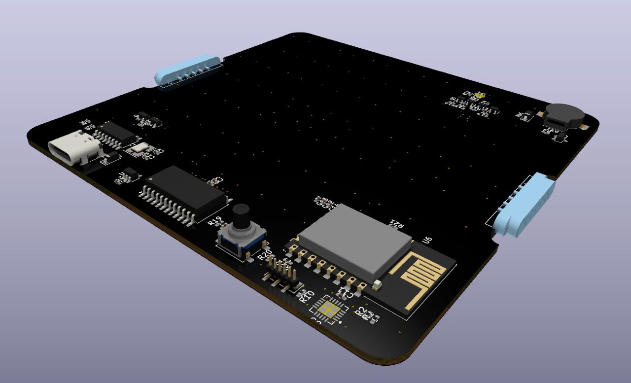
The wifi link (ESP32) isn’t actually an ESP32. I had a look at what I actually had and it was a D1 mini, which actually has an ESP82266MOD with 4MB of flash (over the SPI pins of the dev board, so those are actually out of action). Now, these are pretty cheap on LCSC, about $2.5 or so. The “dev board” is an ESP12F - really low GPIO count, and not many bells and whistles. It needs a USB 2 UART, a few pullups/downs, and a 3v3 LDO.
-
I realised that, to keep costs down, I should make a PCB with all components on every module (IE, wifi, LEDs, USB connectors, etc.) Obviously only one board (let’s call it, the master board) needs a wifi module/USB, etc., but I can reuse the same PCB board for each. That way, I can get 20 ish made at JLCPCB, probably 100x100mm, for like $20.
23/02/2026
So I want to think about the current requirements of the LED supply.
Since it’s rastered (that is, column driven) I think the worst case current, assuming full brightness, would be \(8 \cdot 20mA = 160mA\). But, that’s for just one module. We have 15 (maybe 16, seems like a more rounded number? Let’s go with 16 for now) so \(16 \cdot 160mA = 2.560A\). At 5V, that’s about 12.5W - I will just pull this from the USB port that this will be connected too.
24/02/2026
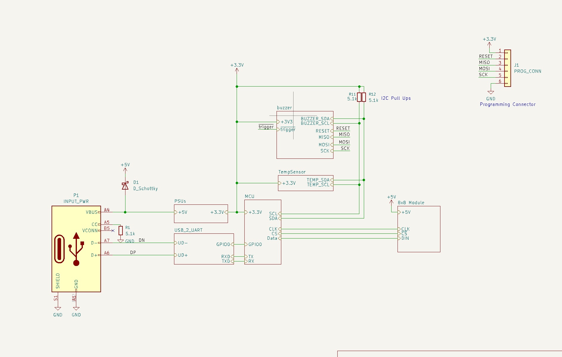
Okay, so, I think the schematic capture is pretty much done. Here’s a pdf of it, in it’s current version.
As I move towards the PCB layout, I want to give a little thought to the mechanical design. The PCB itself will be 100mmx100mm - but how that’s housed, how the LEDs are situated and how far apart, etc., needs a little thought. I know I want some way of passing the 3 display signals (CLK, CS, and data), plus power and ground, in a way that’s easy - no cables. So, that leaves contact connectors (like pogo pins) or some push-fit type connectors (like header pins, but probably something a bit more robust).
Let’s brainstorm:
| connector type | Pros | Cons | Cost | Link |
|---|---|---|---|---|
| Pogo Pins | * Press fit * Cool * More tolerance in X and Y (depending on type) * Intergrated magnets |
* Current carrying capabilities is limited though I found one for 2A (could probably do 2.5A at a push) * Requires manual soldering |
~3$ per pair | https://www.lcsc.com/product-image/C41361293.html |
| Mechanical Connector | tigher fit, might not shake loose on wall. * Cheap |
|||
| (basically pin headers) * Doesn’t require manual soldering (probably) |
||||
| 0.10$ | https://www.lcsc.com/product-detail/C18357552.html?s_z=n_pcb%2520interconnect%25205%2520pin |
So, I really wanted to go for the magnetic one, but all things considered, a mechanical connector makes the most sense. Also, I can reuse the USB connector that I need anyway, so that keeps the overall BOM list smaller. I have an idea for how to set these out physically:
25/02/26
Okay, so I didn’t get a chance to finish where I was last night. I woke up extra early today (0530 hrs!) to have some time to work on this, and other things, before work. I found a nice “PCB edge” connector that I think will work really well for the module interconnect. Specifically, it’s this one:
So, this is designed for PCB thicknesses of 0.8mm. I’ll need to remember that. Gemini seems to think this may not be the best part (and also, I can’t find anything similar on LCSC!) and I need a mid-mount part. So, let’s take a look at those.
Actually, talking a few hours later, I don’t think I need a mid-mount part. I can have a normal mounted USB C connector, with PCB pads on either side. Depending on whether I want to pass USB power in, or pass through the CS, Data, etc.,. I can either solder it from top or bottom, or I could just have 0 Ohm resistors for selecting what goes where - like that idea better, I think. And with that, let’s CAD something simple up.
Quick CAD Model
Nope, no CAD. I flip-flopped back again. I realised an issue. Male USB C connectors don’t seem to be easily available in right angle mounted horizontal connectors. Maybe they are and I’m just not looking correctly. But the more I look at it, the more I would need to either choose both edge mounted, or both normal mounted, to ensure alignment, and I just don’t think I can find that. I’m going back to the nice mag connectors.
27/02/26
Okay, been a couple of days, I’ve been working on a seperate project (inductive charging but let’s refocus on this, and try and get that CAD mockup done of the connectors.
Step 0 - model them because I can’t find a model online :(.
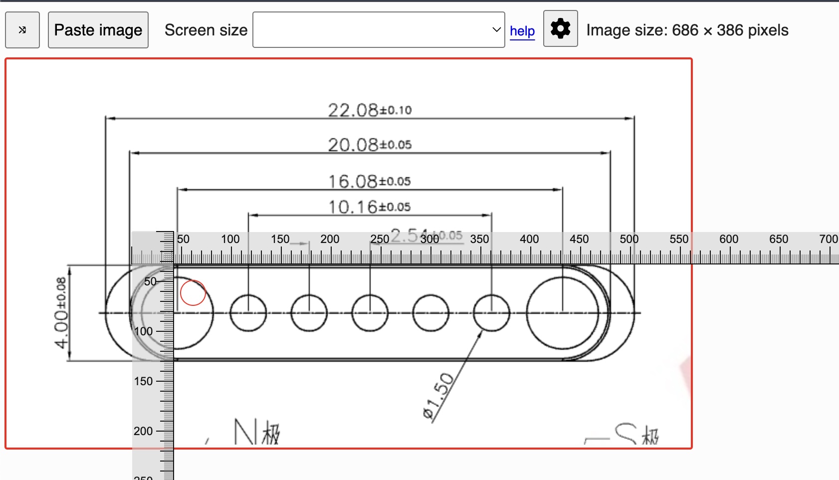
The magcon didn’t have a dimension for the hole which houses the magnet. I used a known dimension (the 4mm radius) and measured the number of pixels. It was 130 pixels. Then I measured the unknown dimension, which was 103, and that gives me:
\[\frac{4}{130} \cdot 103 = 3.16 \approx 3.2mm\]So now I have the dimension!
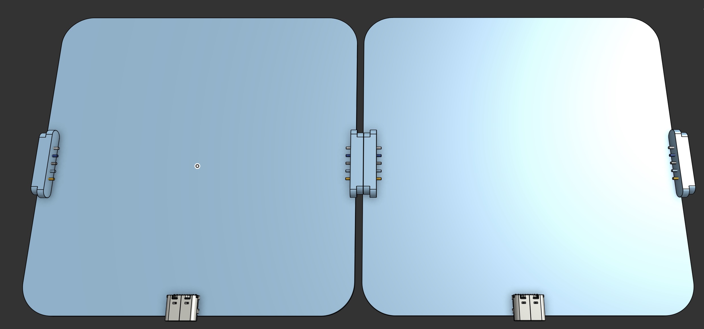
Okay, so I got the connector modelled, and I started place them on the “PCB”. This will be the basis for me to understand how the enclouser will look. The enclosure will house the PCB, but also the LEDs and possible use some lithophane type techniques (or not really lithophane, but some type of dispersion maybe?) of the LEDS. Or I might just have a hole – not sure yet, that’s why I need to CAD it up!
01/03/26
We have a model! A very basic one, but we have a model. This was a pretty decent exercise. I now have a PCB board envelope to work with. I do my modelling in OnShape. It’s pretty easy to get a DXF of the layout, which I then import into KiCAD as a board layout:
Schematic update
I remembered, I wanted to have a buzzer so that I could also use this as an alarm, maybe even play some crappy music. But, I have no pins left on the uP. So, I do have an I2C bus, but I haven’t played or seen any I2C buzzers before. Let’s see if I can find any.
Okay, I had a look, all I can find that’s somewhat decent is the SparkFun speaker board. It has an ATTiny84 on there for basically being an I2C -> PWM converter with configurable frequency and volume. I checked LCSC, it’s like 2$ for an attiny84 and then another few dollars for the buzzer, which is currently out of stock so I’ll probably chose a different one.
For the sake of a couple of dollars, I’ll add one (of course, the footprint will be on every module, but only one can be used unless I pass I2C bus over the modules some how. I’ll need to write my own firmware for it, but that’ll be pretty cool. I have this old programmer from SparkFun that programes the ATTINY series, so I can easily program it that way. Seems like a pretty cool addition. Plus, the schematics are all available, so nice and easy.
Let’s add this to the current schematic and update the github repo. Then, we’re ready for PCB Layout!
Ah - I just found this which is the firmware for the attiny! I might need to make mods, because the pin out may not be the same (I might use a digipot for the volume) but that will make this much much easier!
In the end, I didn’t go with the digipot. LCSC has a bunch, but I’d need to mod the firmware and now I know I don’t have to write custom FW, I’m lazy! The pinout for the IC I’ve chosen (QFN) is not the same as SparkFun’s, so I’ll need to do some pin changes, but that should be fine.
Schematic’s not finished, but I’ll do some more tomorrow.
02/03/26
New day, let’s gooooooo.
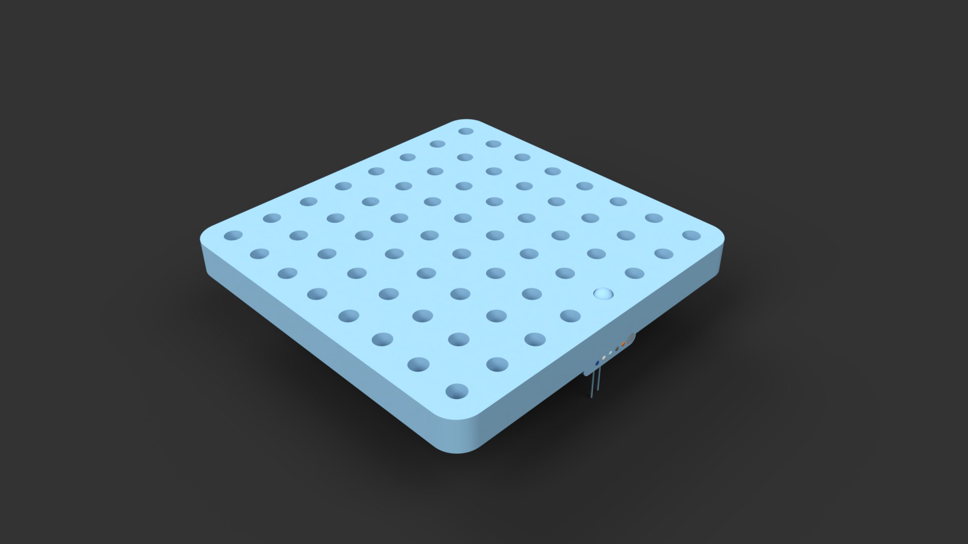
Alright, I added a buzzer, it was pretty involved, but it’s now done. Back to the PCB. The exported PCB board file is nice, but I would like guidelines on where to put them. Luckily, we can export that from OnShape, and add it on a layer in the PCB.
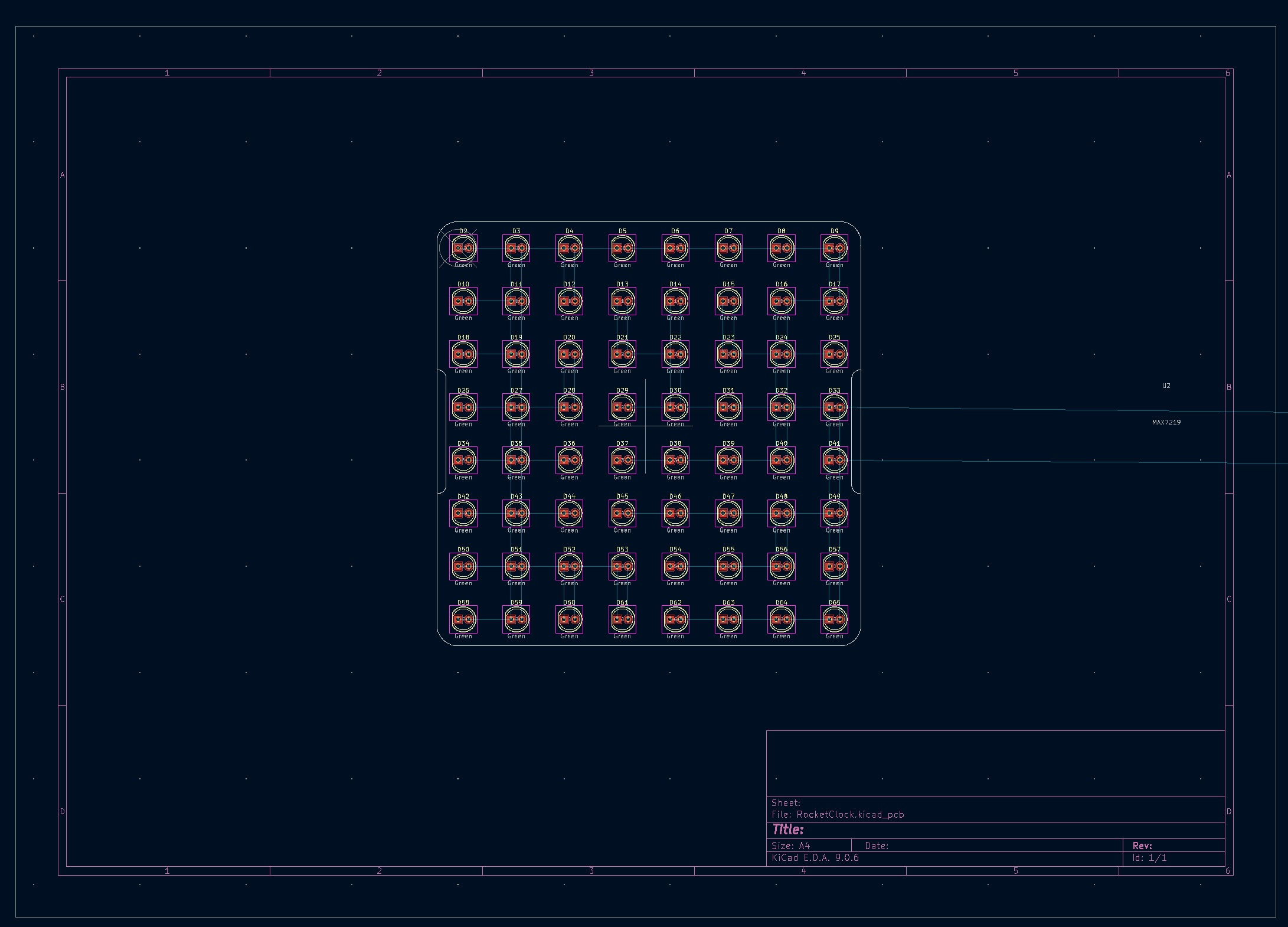
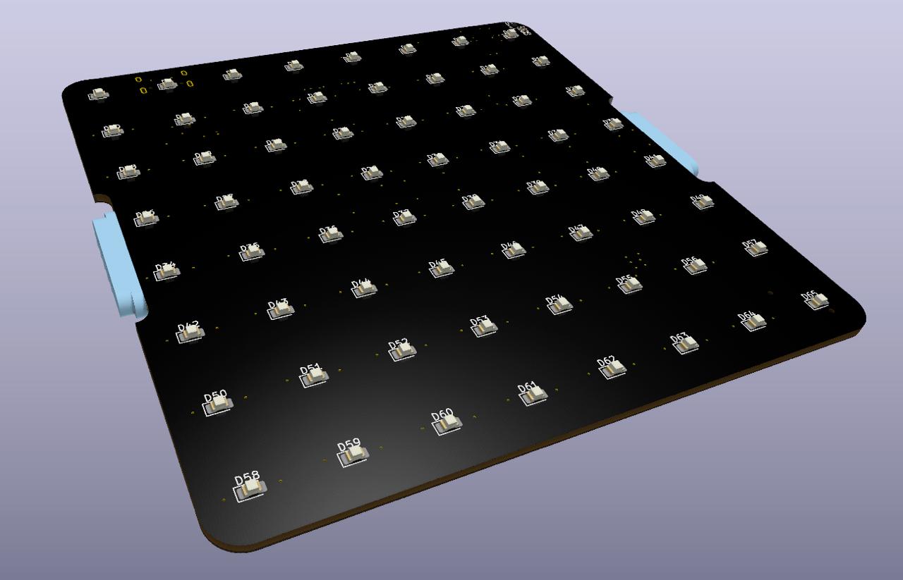
This was actually pretty easy in KiCAD. I used the DXF of LED places from OnShape to understand whereabouts I need to place them. Then, I used the Grid Array feature in KiCAD (CMD + T on a mac) and placed them in an 8x8 grid, with 12.5 (\(\frac{100}{8}\)) spacing.
07/03/26
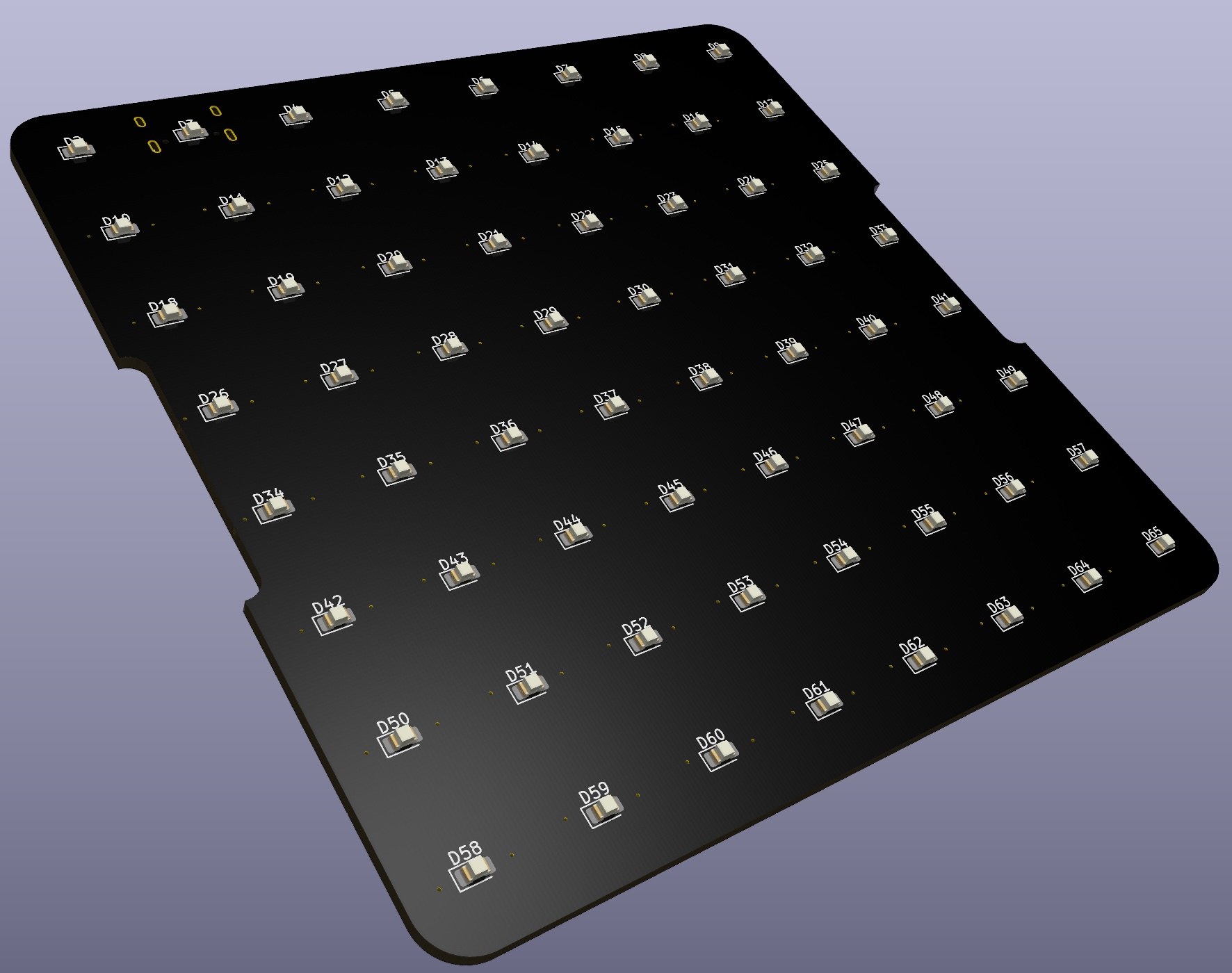
Quick update: I’m an idiot. I wanted to use through holes to give the modules an archaic feel, but that’s not going to work. There’s so many holes that I can’t place anything on either side of the PCB. DOH. So, I’ll update the LEDs to SMD (they’re cheaper, too!) and then maybe we’ll need light pipes or maybe we can get away with just the 3D printed diffusers or something. Needs some thought, but today (later) I’ll update the schematic to change the footprints to SMD. Sigh.
10/03/26
Been 3 days, not had too much time. I had a couple of issues I wanted to note down though.
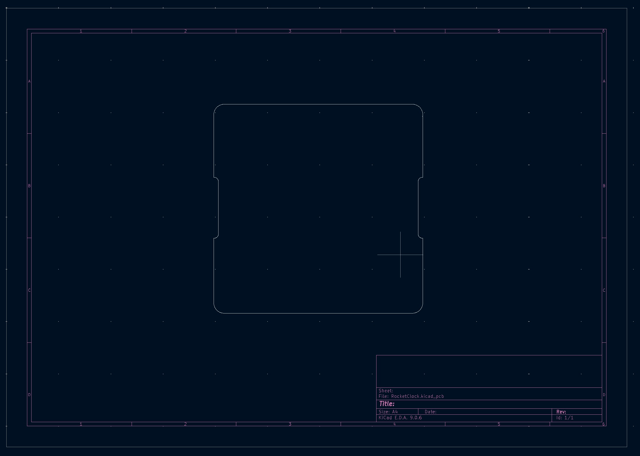
- Edge cuts. I had a small issue with the board outline, easy fix, basically there was a spur coming off the perimeter, don’t know why but deleting it fixed it.
- Replaced THT LEDs with SMD, this means a redesign of the enclosure, at least the holes. Not sure how these will look in real life, probably I will make a test square piece with several types of holes and diffusions, and I’ll see how it looks with an LED before committing to the hole thing
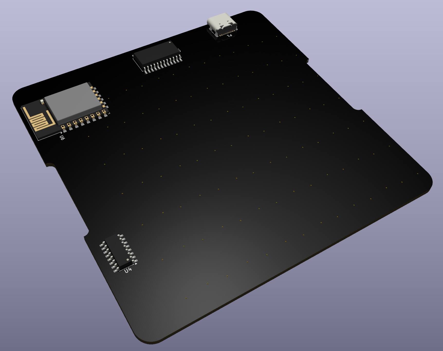
- Finally, the layout of the multiplexed LEDs isn’t the most conducive to a 2 layer board. I need vias to jump over/under traces, but then I litter the bottom side with areas where I can’t place large components. I do have these areas near the top and right of the board where there are no vias or bottom traces. I’ll try and fit most components there.
Anyway, that’s all I can update today. Hopefully will get some more time for this later this week, and get the boards made! It’s been about 5 weeks since I had this idea, so need to get the cadence up!
16/03/26
I’ve mostly done the layout now, I wanted to add some photos to show the progress.
21/03/26
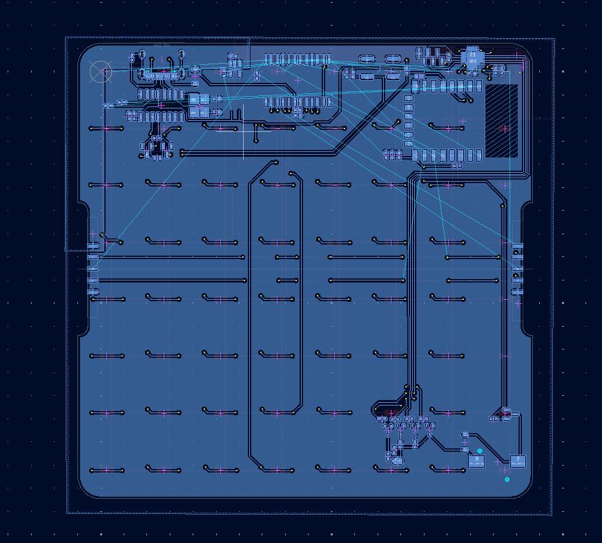
Layout is now done, DRC is passing, and DFM checks on JLCPCB are good. A few warnings about annular rings and some other such stuff (silkscreen over board edge, but that’s not an issue, just how I placed my custom magconnector footprints).
I’m using Claude to help speed up part selection - when LCSC’s BOM uploader tool can’t find a part (or it’s out of stock) I get Claude to find me a replacement, drop in. For example, the buzzer I used was available in LCSC, but it’s out of stock. Claude was able to find a great match, based on a bunch of metrics (DB, size, footprint) and one that’s in stock - I was pretty impressed!
25/03/26
Okay, so, about 2 days ago I finally hit the button on the order! The grand total is:
- PCBs - $94.08
- PCBs (x30) - $30.40
- Shipping - $45.47
- Customs - $18.21
- Parts - $ 152.58
- Parts - $135.38
- Shipping - $34.82
- Discount - $17.62
Total: $246.66
So, it was quite a lot! But, I did get enough for 30 boards. The mag connectors were not in-stock which was a shame, so I had to order some header pins (luckily the mag conns were 2.54 mm pitch parts and I made a custom footprint (to solder them parallel to the board) so it was an easy fix)). Shame I can’t easily extend the modules, but it’s okay, I can buy them later if needs be.
All the board files, manufacture ring data, bom, etc, are here. I haven’t started the software/firmware yet, I wanted to think about that a bit here.
Software
I think I’ll need:
- Rocket Clock Server, this will technically run on the ESP12F.
- Also, turns out the ESP can also serve webpages, simple ones that is. So, that makes things more simple.
- Attiny FW, this is already written for me by SparkFun, so that’s easy
It’s actually pretty simple, in my head there was a lot more I needed to do. I have an ESP12F here so I can start on some of the work, things off the top of my head:
- UI interface, to be served to clients, to do the following:
- Events
- Set Alarms / Clear Alarms
- Tell me next rocket launch
- Word of the day
- News
- My next calender event
- Take a character, for example “a”, and convert to the required LEDs to illuminate on the module
- Horizontal scrolling of text
- Vertical scrolling of text
- Temperature reading and display
- Pulling in data from outside (rocket launches, weather, etc)
- Buzzer interface over I2C
Anyway, that’s the update, PCBs should be here on 31st March. That gives me about a week to get the software ready, or at least as ready as I can without actually having the hardware!
29/03/26
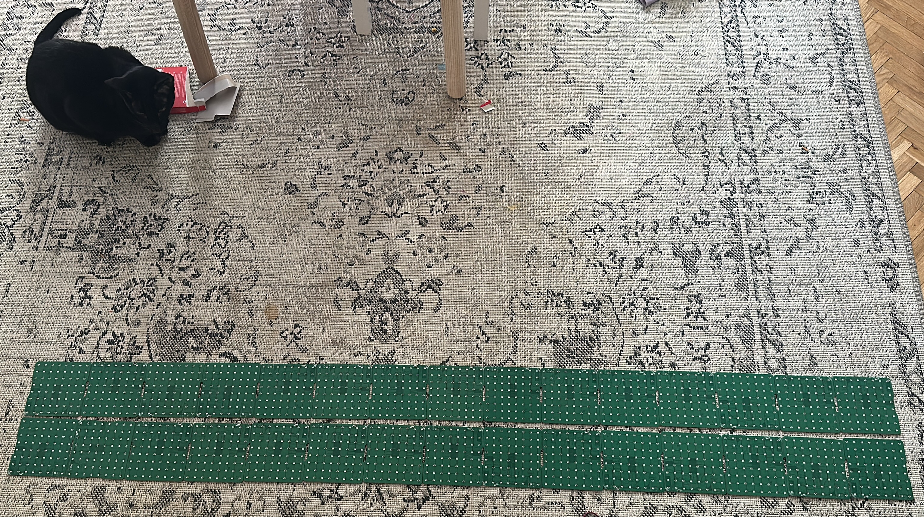
PCBs!!! I got them, check it out. They came several days early, which is awesome. I don’t have the parts yet (they arrived into France this morning from China, so a few days to get over to Estonia).
03/04/2026
I’ve actually done a bunch of stuff here since the last post. I haven’t been able to update here, though. So I’ll do a quick data dump and maybe will write up more in the future.
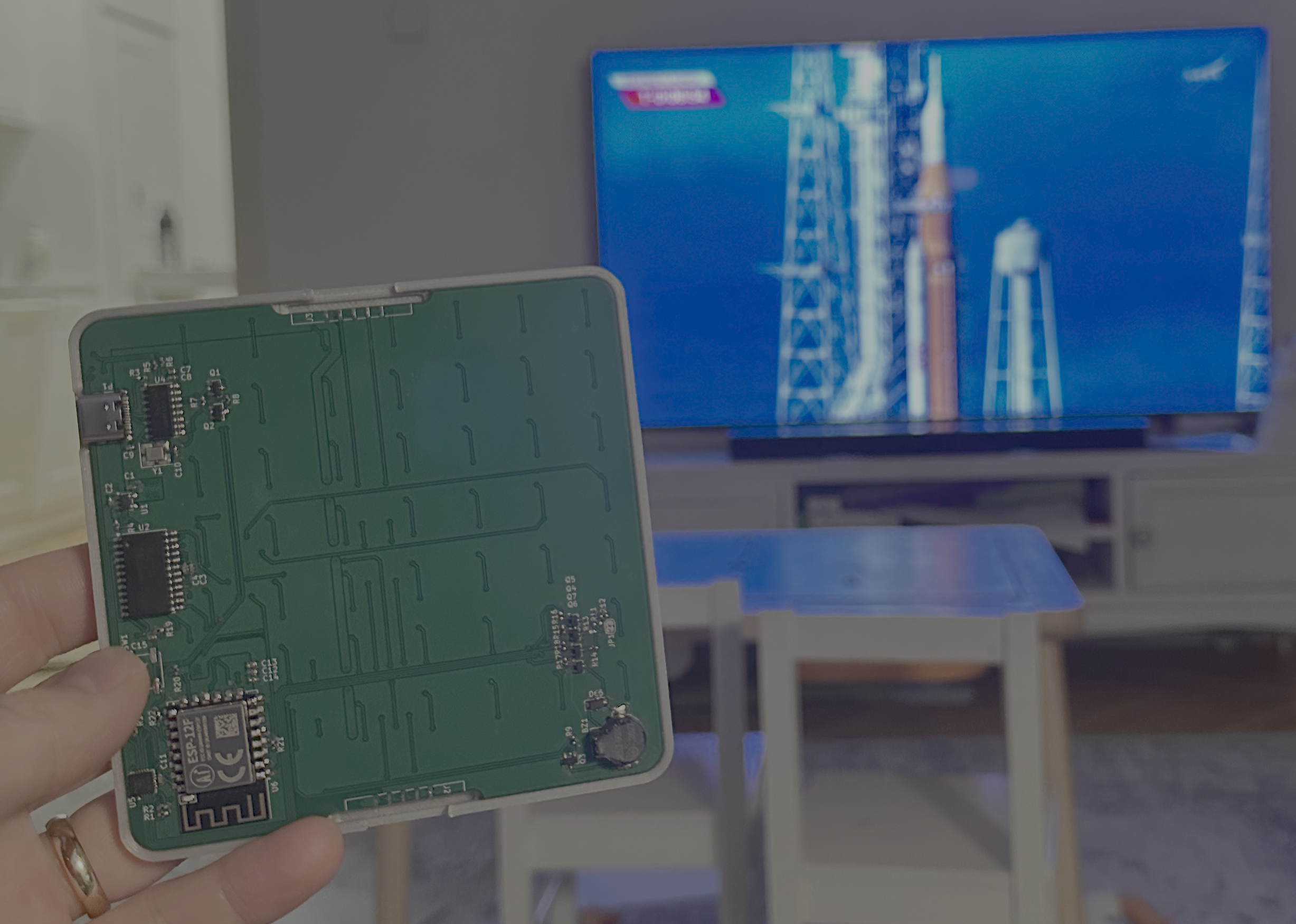
On the night / morning of the launch, I cracked open a monster energy (launch window started at 0130 on the 2nd of April), my daughter went to bed at about 8/9, and I started soldering up my first board:
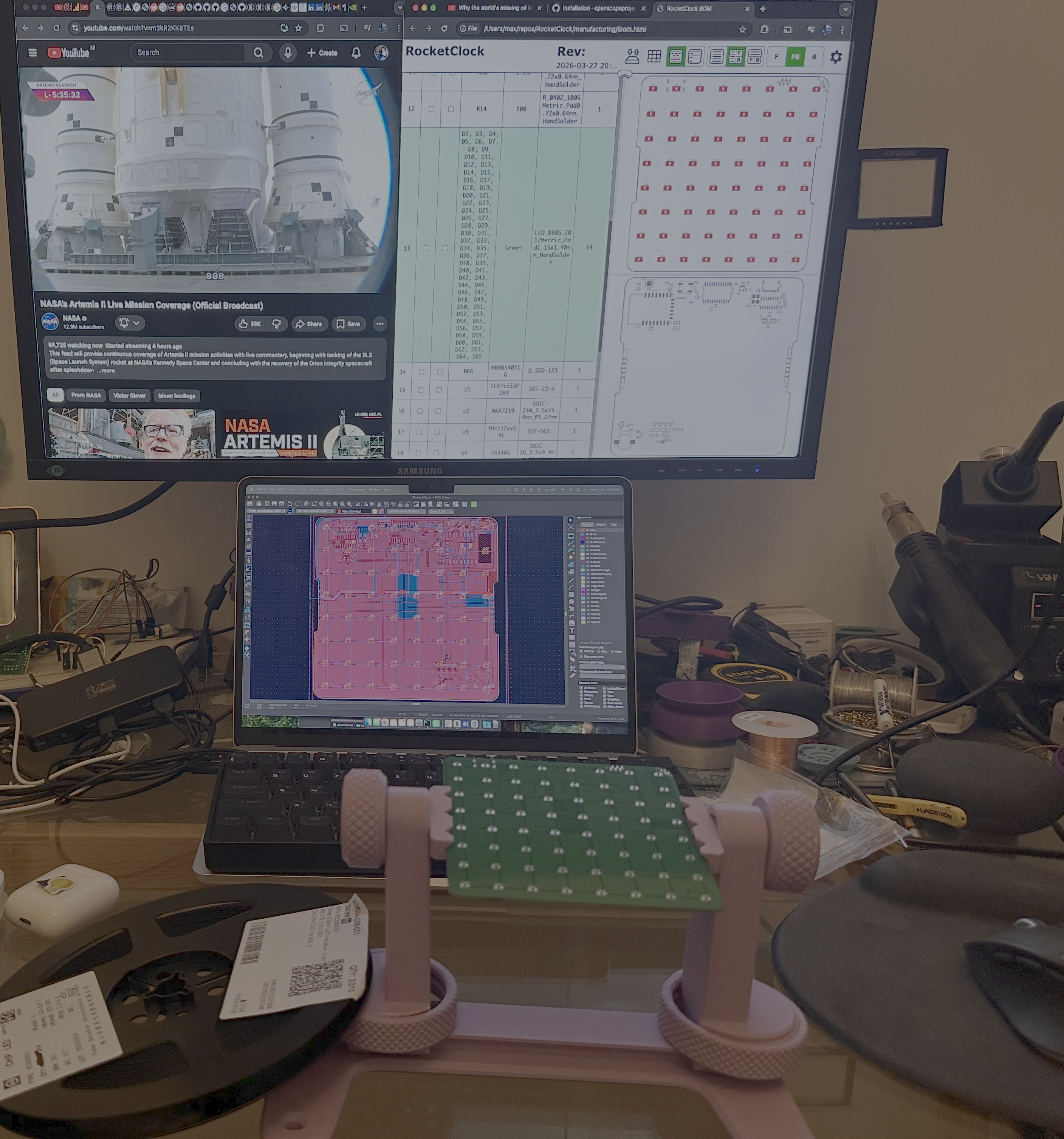
I used the IBOM of the board, a super nice plugin that allows a view of the BOM (which helpful tick boxes), then the cross selection of item to location on front or back of board (and vice versa)).
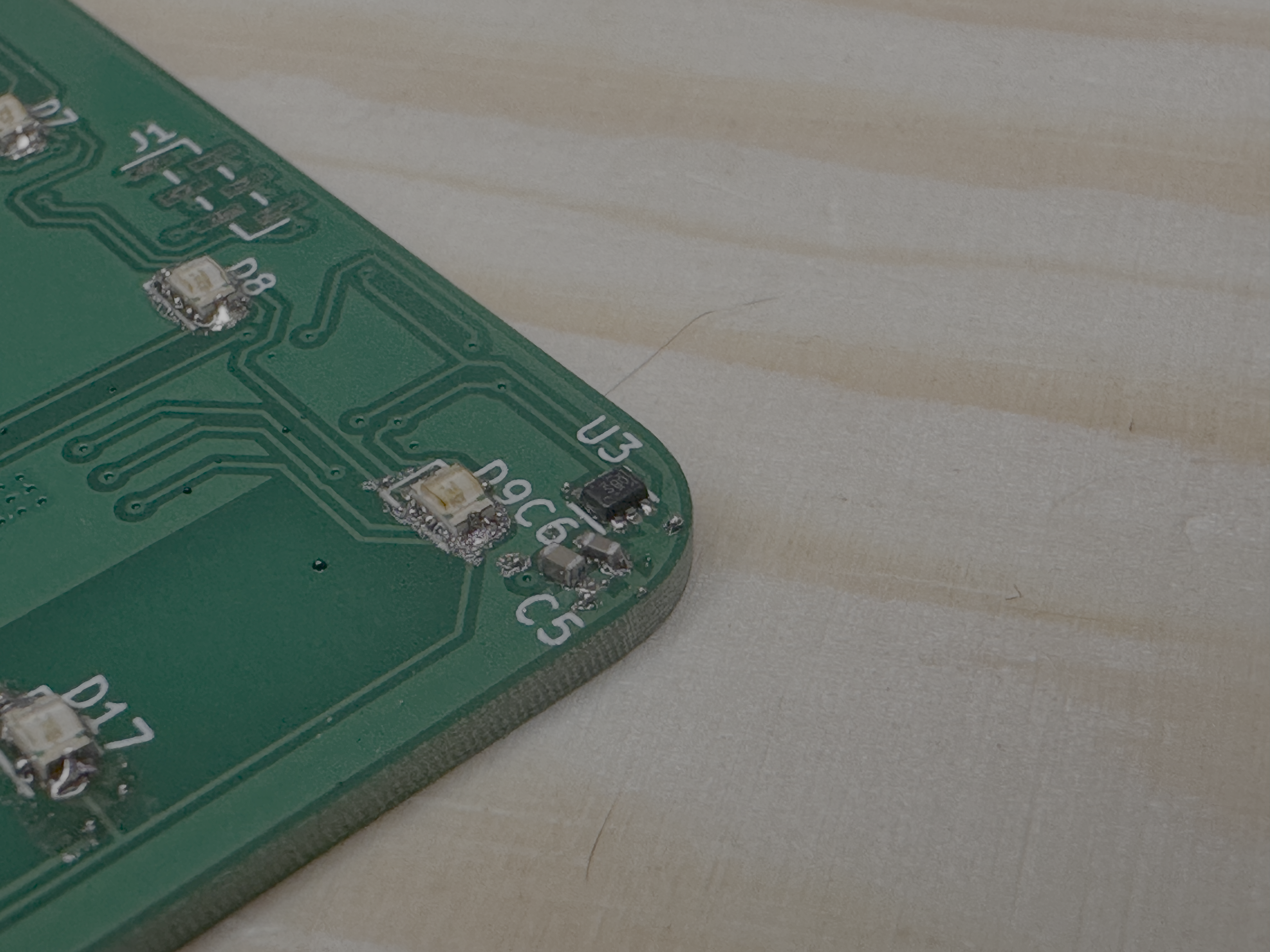
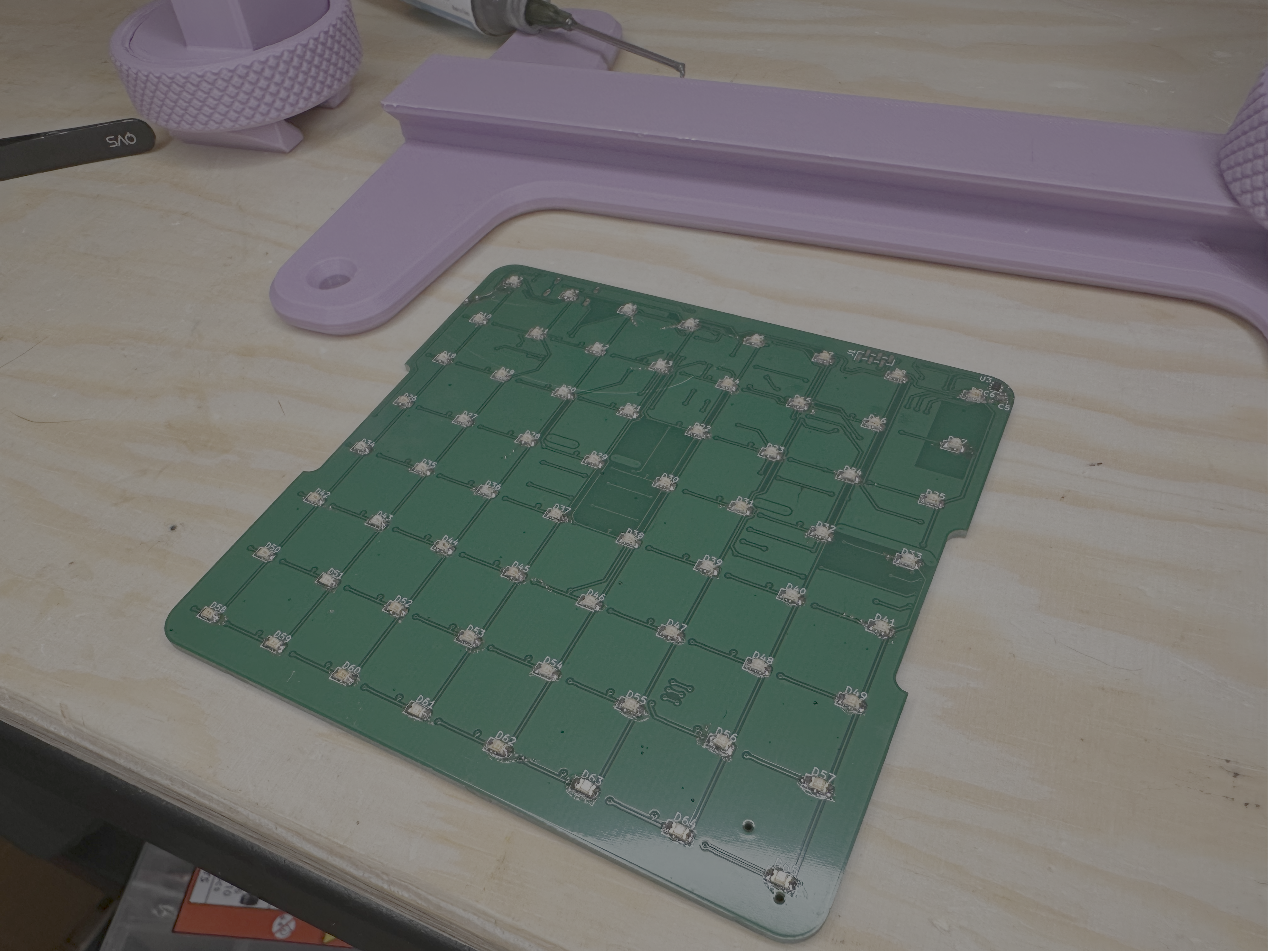
I populated the LEDs first, it was pretty easy to do them, actually. The most difficult part was the temp IC - small footprint to paste without a stencil.
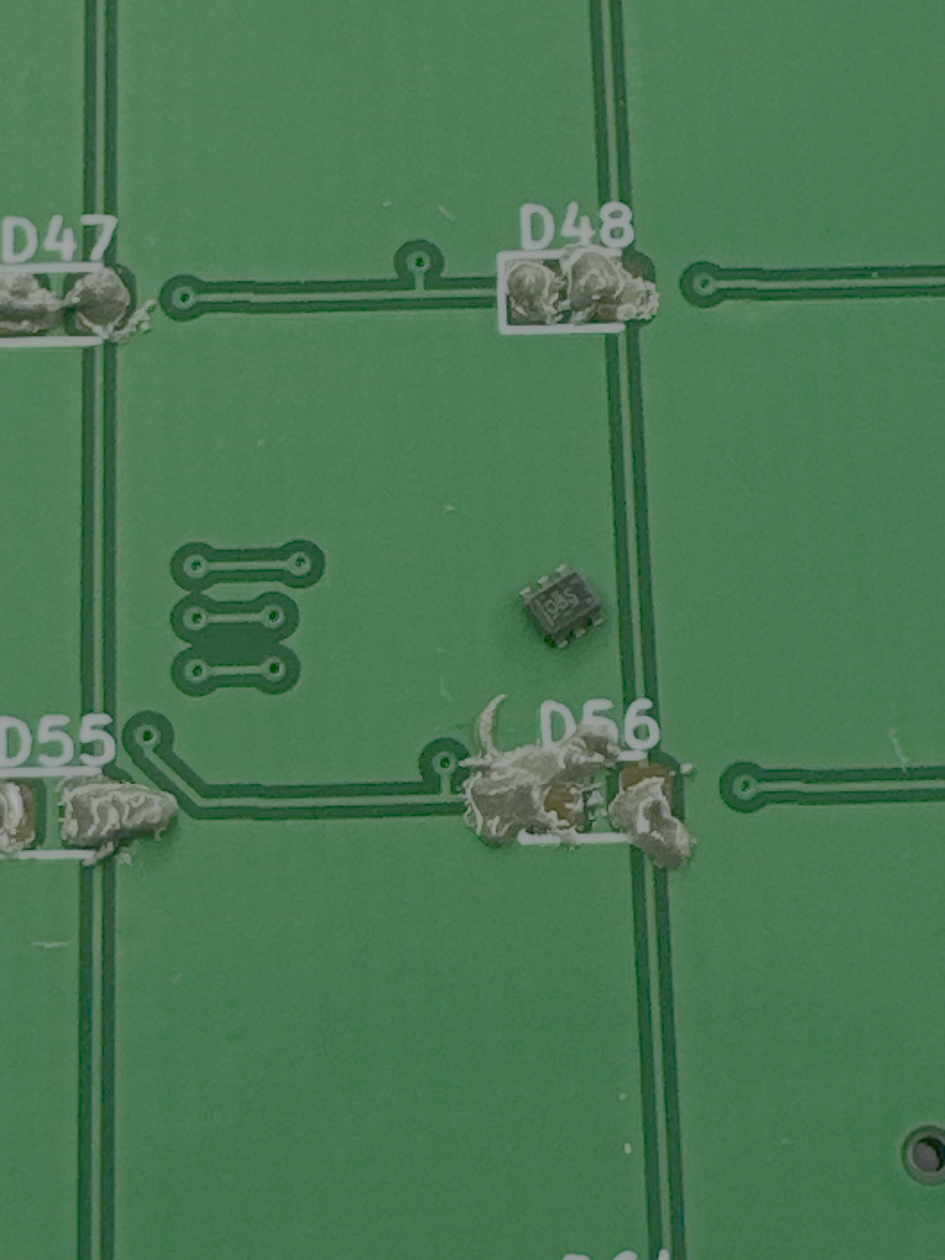
The solder paste was a little messy, I just squeezed it with the syringed paste. It worked, though. I did touch up all LEDs after, just incase. I also had one LED (you’ll see in photos later) that didn’t solder, and one that fell off when I dropped the board 🤦🏻♂️).
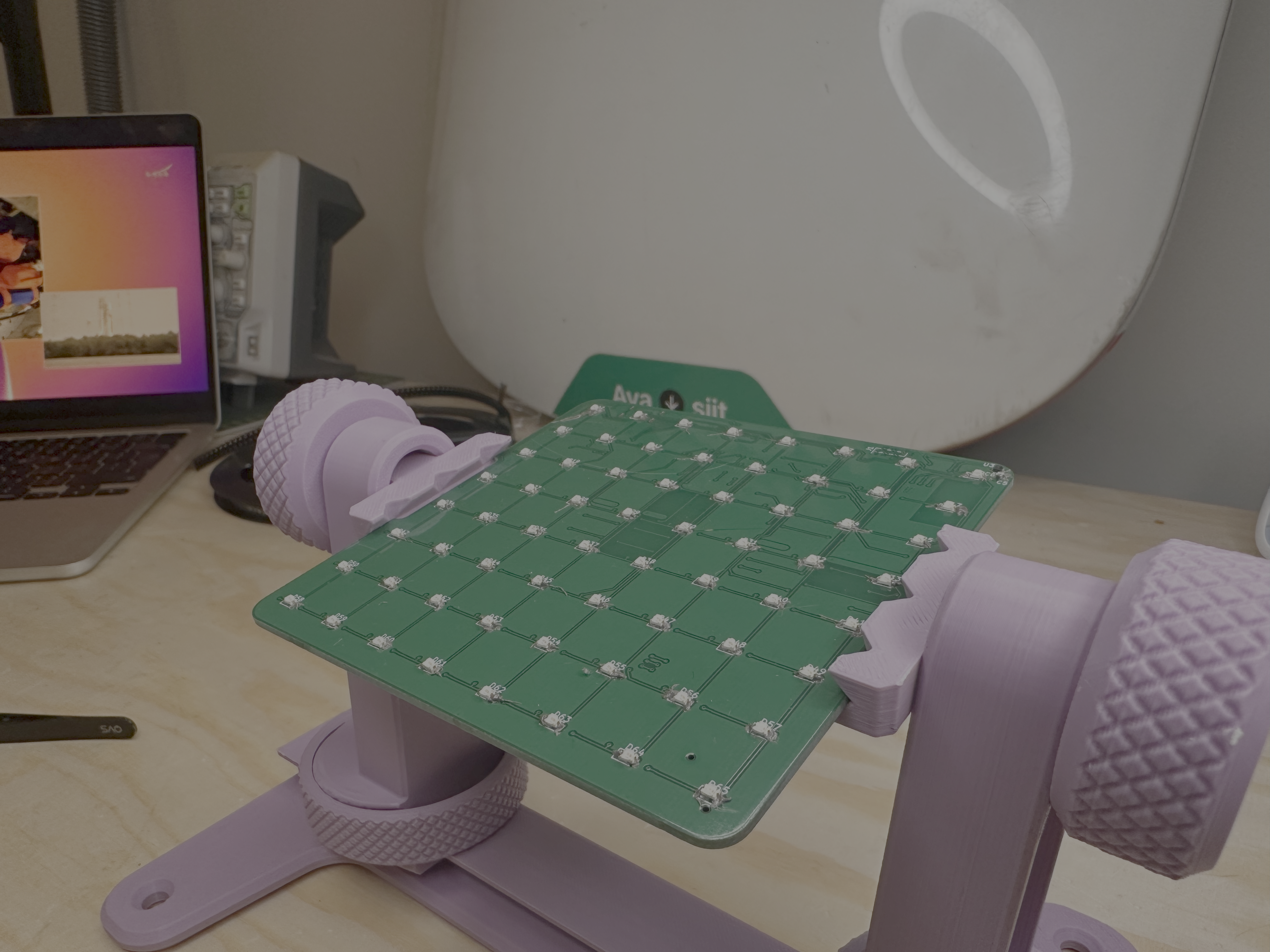
That’s the LEDs populated before I used a hotair gun to solder.
It didn’t reflow well. That could be because of a few reasons, I think:
- solder paste was left too long (approx 1 hour after application)
- too hot, or somehow I evaporated all the flux before the solder melted (not hot enough?)
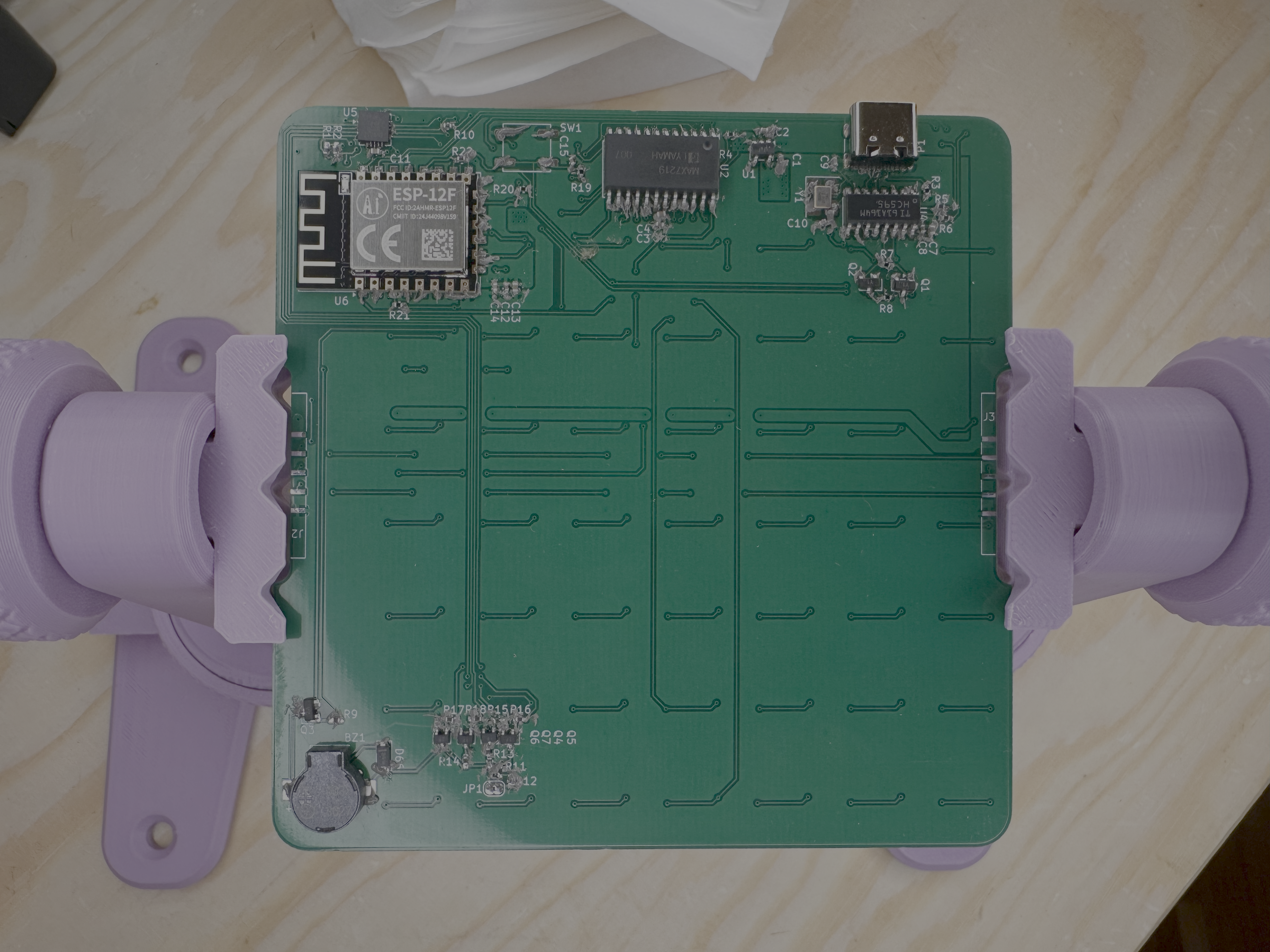
In any case, I touched up all the LEDs and temperature IC, all looked a lot better after that, and I tested most lines using a DMM (using diode function) and the pads from the MAX7219 IC.
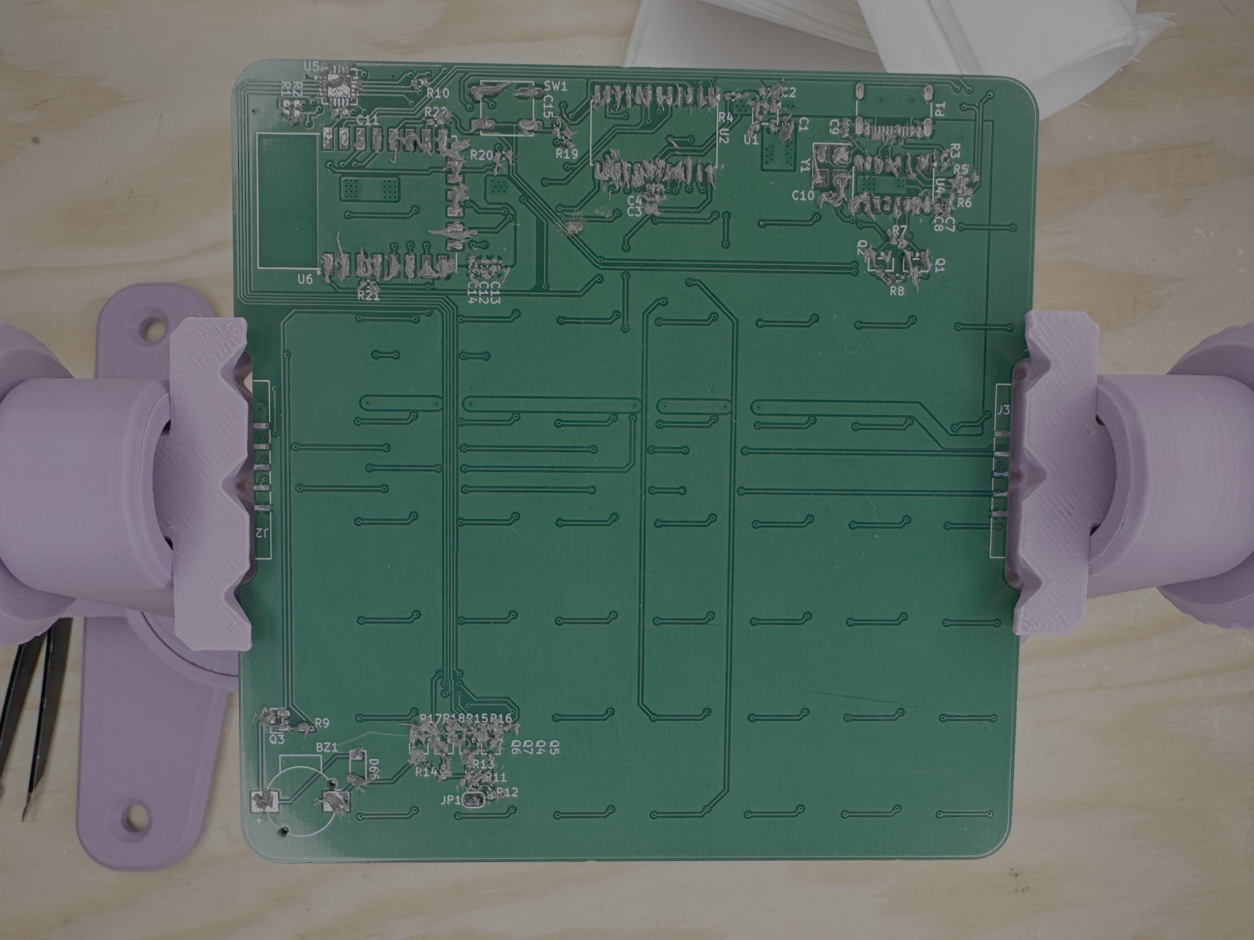
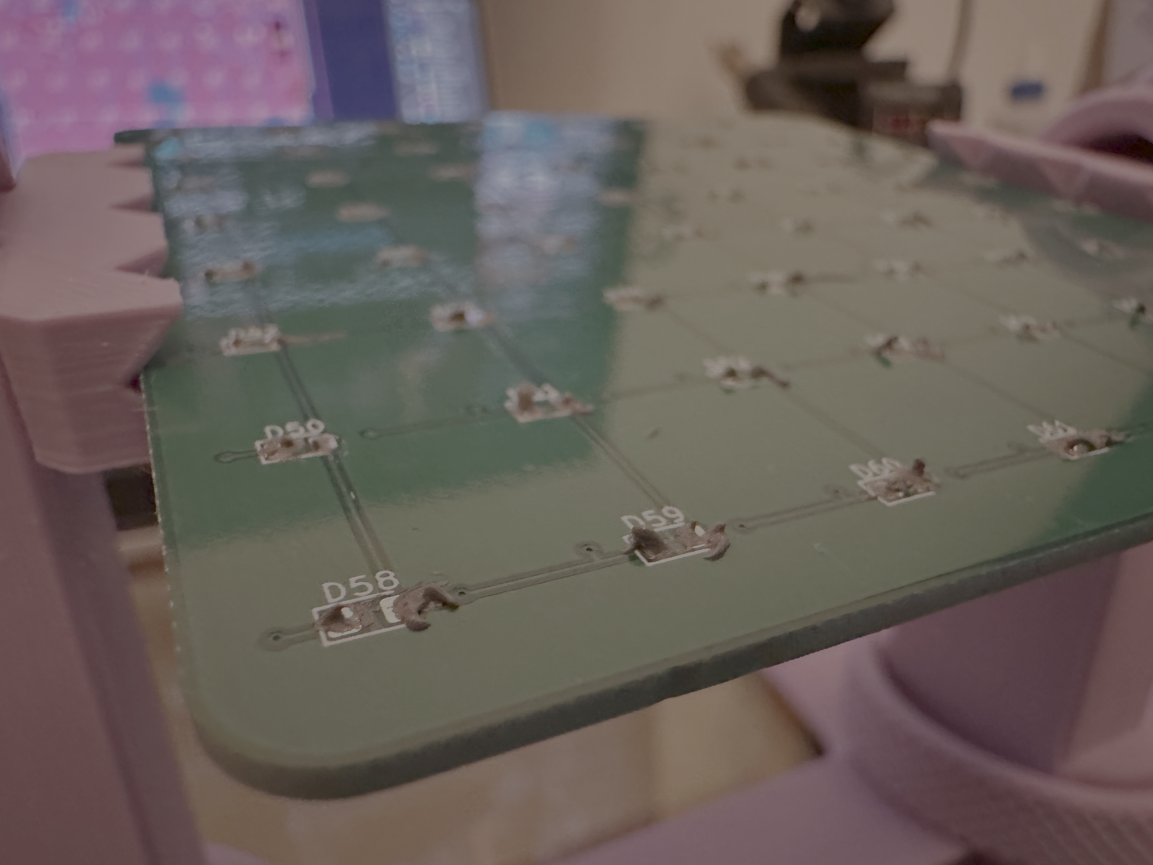
The back was basically the same as the front side of the board, though, it took a lot longer. Obviously a bunch of different components, and a lot of 0402 passives which take a little longer.

A little messy, again, but okay. I touched up each part again with the soldering iron and sometimes with liquid flux to get nice clean solder joints.
At this point it was about L - 15 on the clock for the launch. I thought, maybe, if the board worked first time I might be able to get a simple 10s count down going in sync with the launch - but there was an issue. Spoiler, I didn’t find it until the next day, but look was sleep Max placed instead of the USB to UART IC:
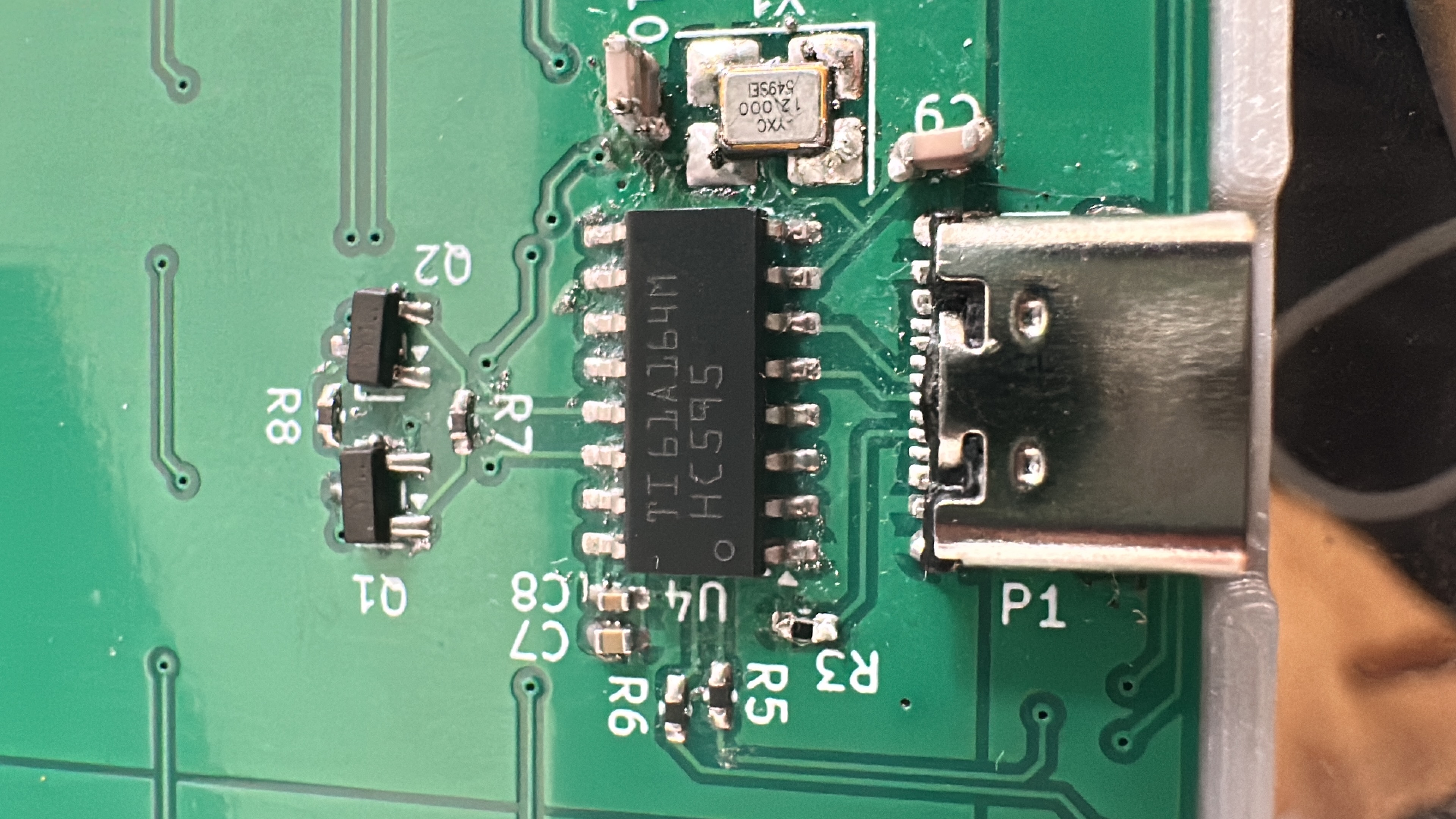
That’s not the CH430!.
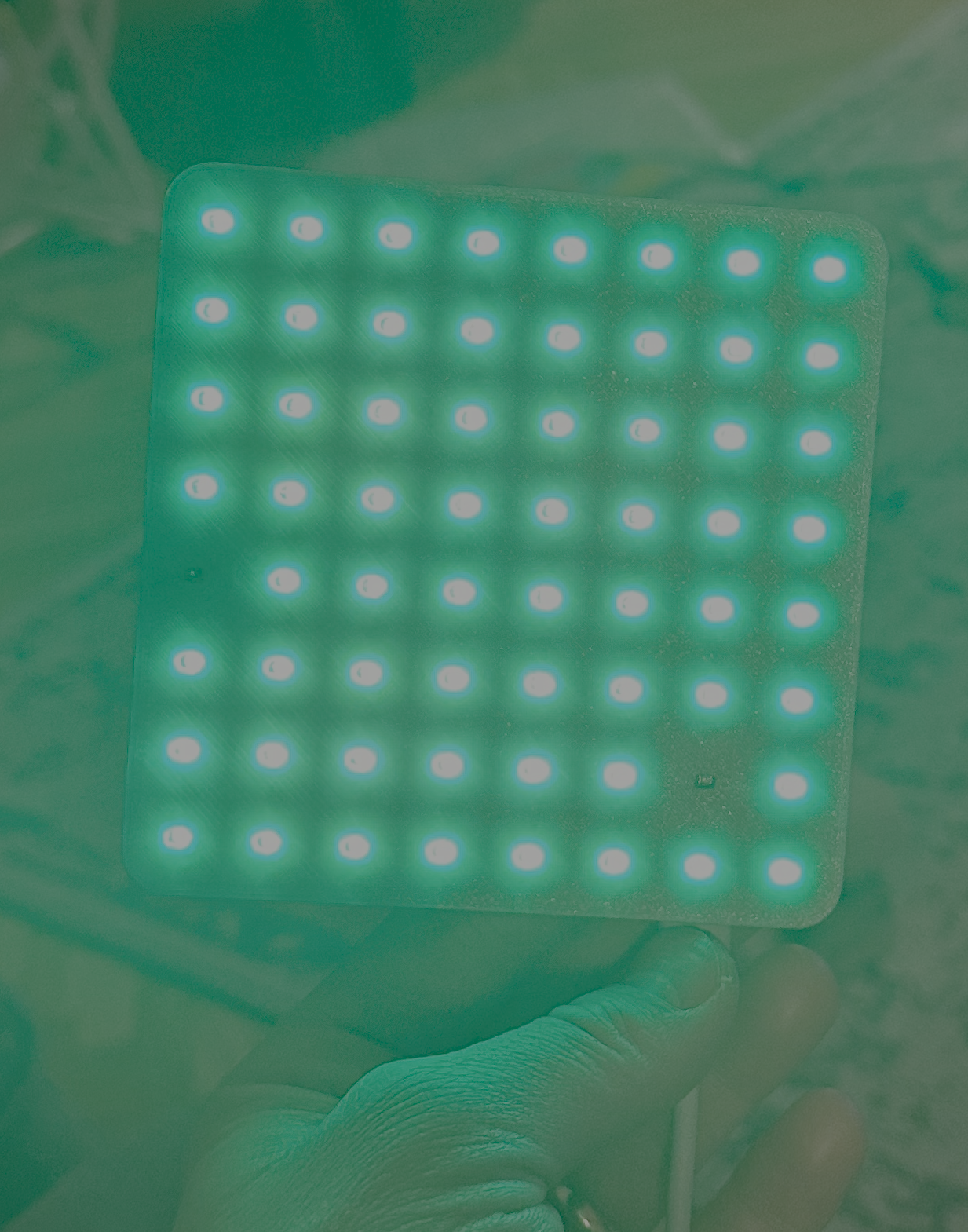
Anyway, the board did light up all LEDs (just USB wasn’t being detected, obviously).
https://youtube.com/shorts/8IFnWLreycE?si=TLuFFuXFJKIlkUf4
I took a super short video of it working (rotating smiley face that I got claude to do).
Currently, I’m working on converting an image into something that can be displayed on the board/s. I have only one board at the moment, so i’m converting images to greyscale, then I will run a kernal over that (sized correctly such that the kernal will run 64 times over an image) and then calc the average greyscale value in that kernal - and threshold it. Anything over 127 will be on, and anything less will be off.